Dual Microwave Source v1
Requirements
After completing the design of the Single Source succesfully, we decided to proceed with a more complex design. For magnetic pulse sensing applications, it is often desirable to have a source, which can provide phase-shifted signals. For example, a pulse sequence requires at least the input of a 90° and 180° phase-shifted signal (Fig. 1.). The big advantage of the presented design over structural phase shifters is the fact, that the relative phase shift does not dependent on the frequency. The following sections describe the design of this solution by usign the resources from the Single Source.
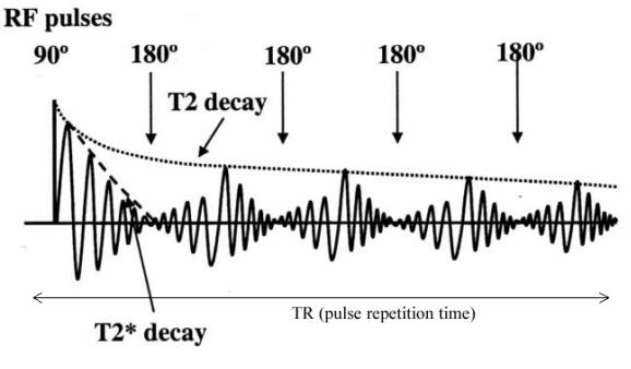
Fig. 1. - CPMG Pulse Sequence - Spin Echo.
System Design
The system consits of two PLL chips, which are locked to the same reference clock. Each chip features a differential RF output which is used to supply a 180° phase shifted copy of the signal. Harmonic filtering and output power leveling for each RF branch is conducted by the basic circuit described in the Single Source section. Due to the high count of required digital control pins a I2C GPIO expander had to be used. This chip controls the state of the RF switches and Power Amplifiers. The synchronization of both microwave sources allows the Microcontroller to program an arbitrary phase offset on one of the PLLs.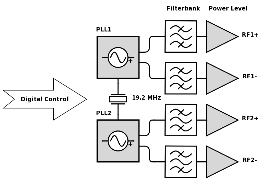
Fig. 2. - Symplified System Schematic. A detailed compostion of the Filterbank and Powerleveling can be found in the documentation of the Single Source.
Phase Shift - Synced PLLs
In order to generate phase shifted signals we use an interesting feature of the MAX2871. Two chips, which are driven by the same reference clock, can be synced by resetting the Phase Detectors (PD) of both PLLs at the same time. This event is triggered by the rising edge of the SYNC signal created by the microcontroller. Unfortunately, this event only can be triggered inside the falling edge region of the reference clock signal. Thus, the microcontroller has to been fed by the inverted 19.2 MHz reference clock. An internal clock selection bank allows to switch from the main 12 MHz clock, required for supplying the USB interface module, to the inverted reference clock source and conduct a sync-process of both microwave sources. Subsequently, one of the PD is programmed to achieve the desired amount of phase offset.
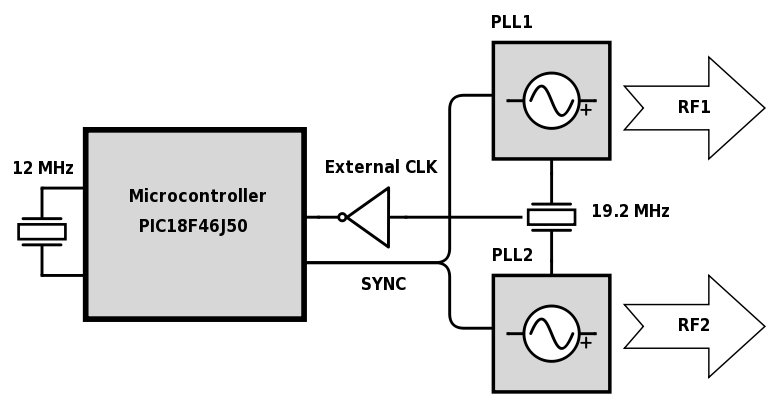
Fig. 3. - Clock architecture of the dual microwave source. The SYNC signal allows a synchronization of both sources running on the same reference clock.
PCB Layout & Manufacturing
The PCB layout is similar to the first version: a 4 layer PCB stackup, 0.34 mm RF track width and no solder mask on the RF signal lines. The RF ground on the top side is isoltaed from the digital ground and the two internal layers serve as distributors for the power supply rails. PCB was manufactured by OSH Park.
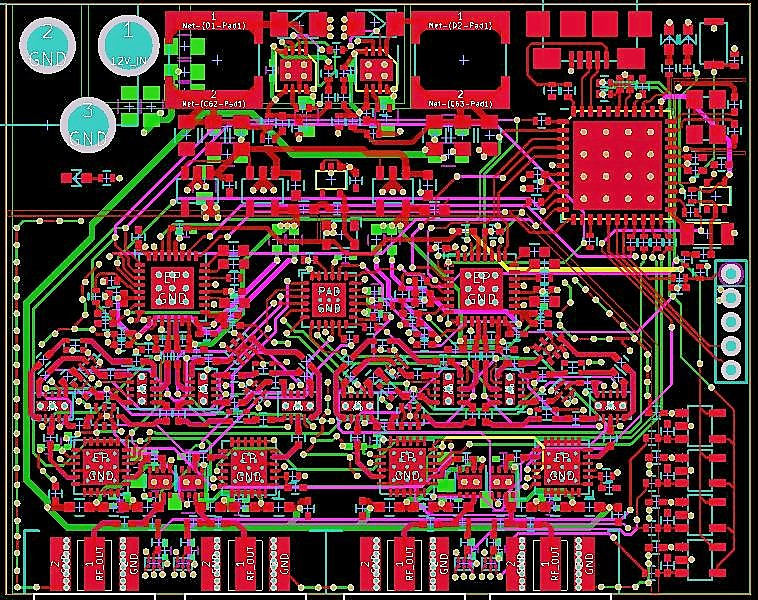
Fig. 4. - Board Layout rendered from KiCad.
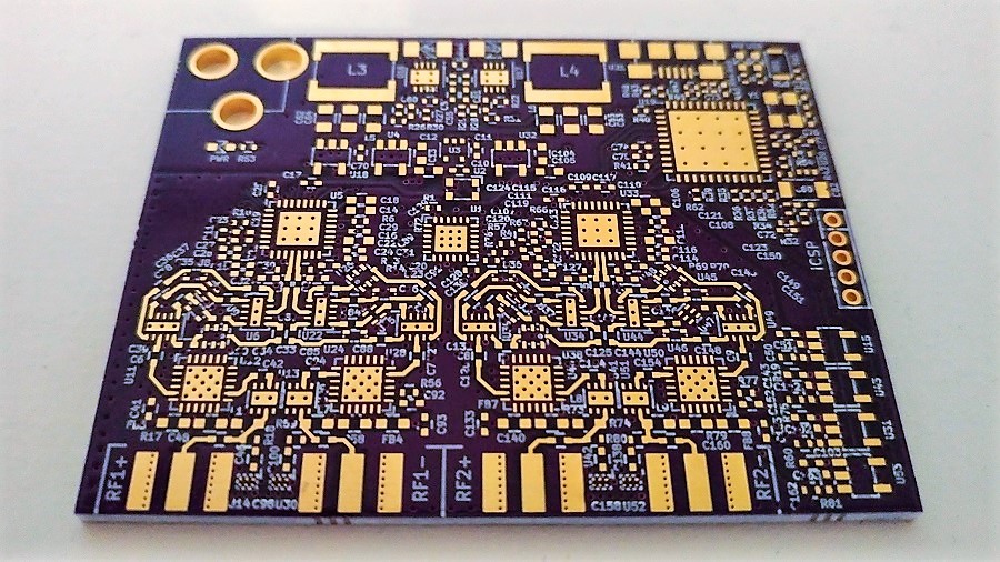
Fig. 5.- Photo of the bare PCB Board.
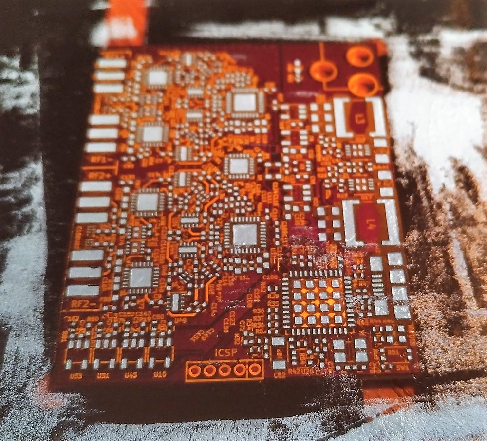
Fig. 6.- Spreading solder paste with a stencil.
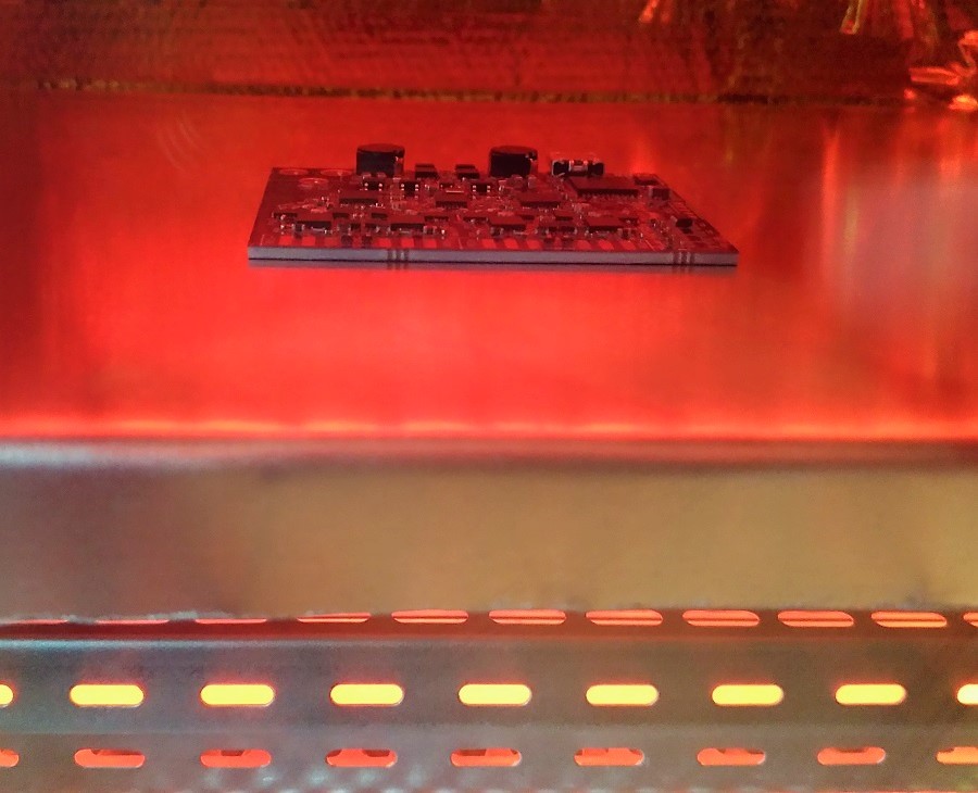
Fig. 7.- PCB during reflow in the oven.
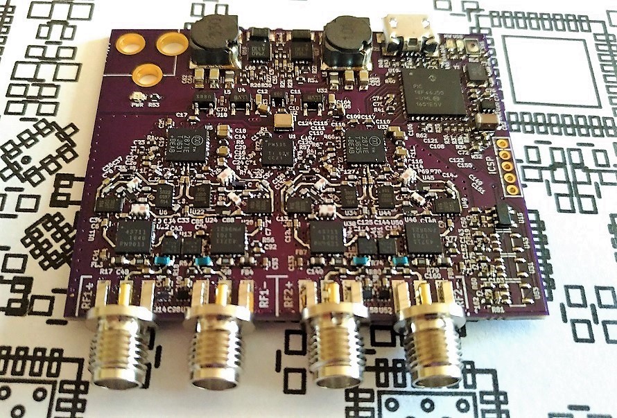
Fig. 8.- Photo of the PCB after reflow.