Spectrum Analyzer
Circuit Design & Schematic
The USB spectrum analyzer makes use of an RF-reciever module and an FPGA to process incoming signals. The RF-reciever first conditions the signal level with a programmable attenuator / LNA and subsequently downconverts it to an intermediate frequency using an active mixer (ADL5801) and a local oscillator (MAX2871). After being downconverted, the IF signal is filtered and digitized by an high-speed ADC (LTC2247). The digital signal is then processed with a Xilinx FPGA (Artix-7) and results are send to a PC via USB. The communication with the PC and the programming of the FPGA is handeled by the FTDI FT2232 chip set.
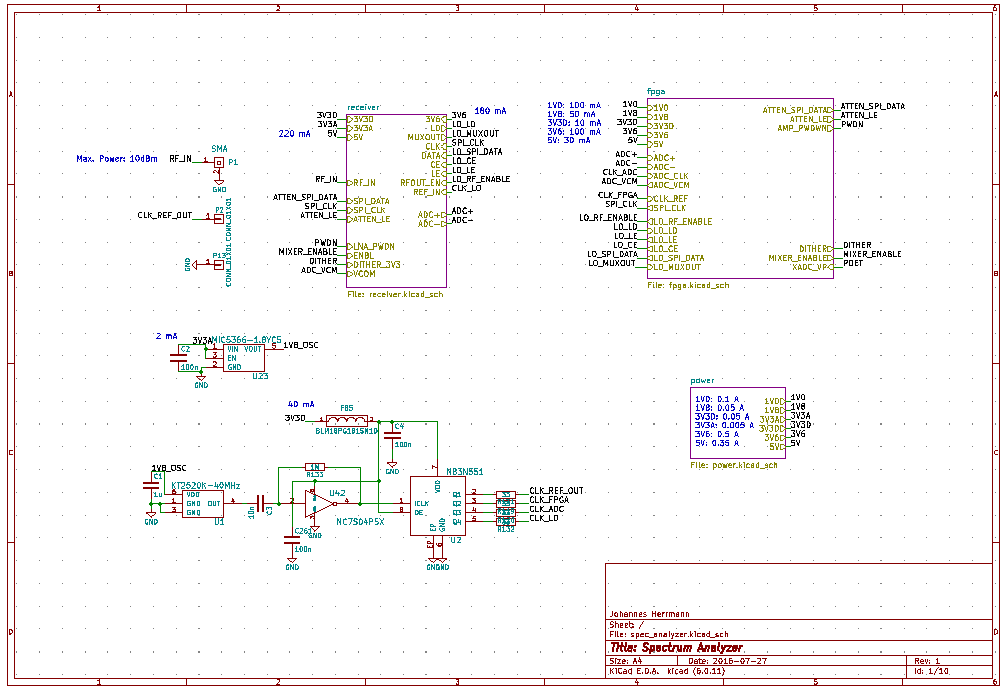
Schematic. Click for PDF.
Board Layout & Manufacturing
The layout is deployed on a 4-layer PCB stackup and shields the RF part from the digital circuitry using seperate board areas. The board has been assembeled with an homemade reflow-oven, see Fig. 2.
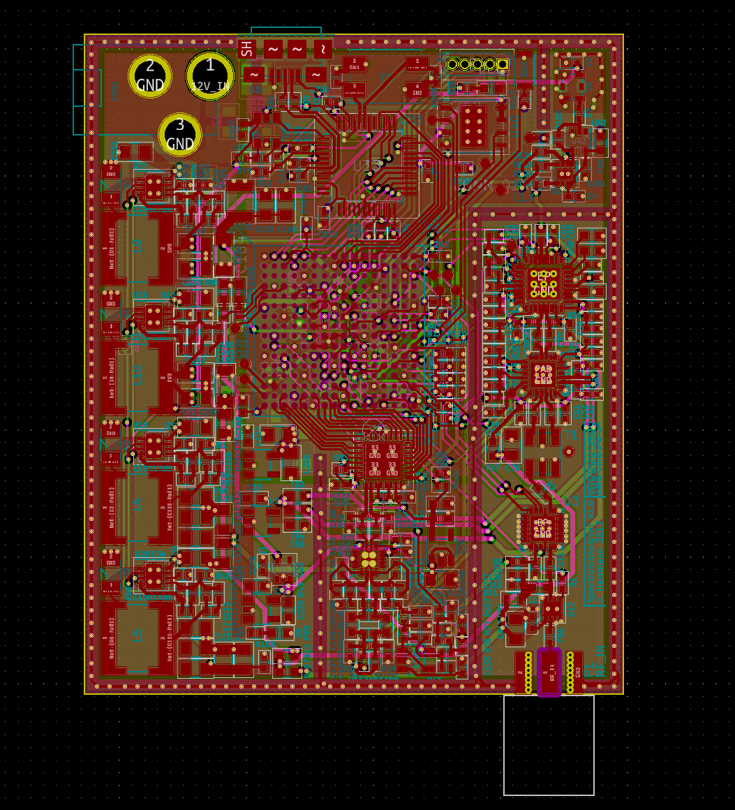
Fig. 1. - Board Layout from KiCad.
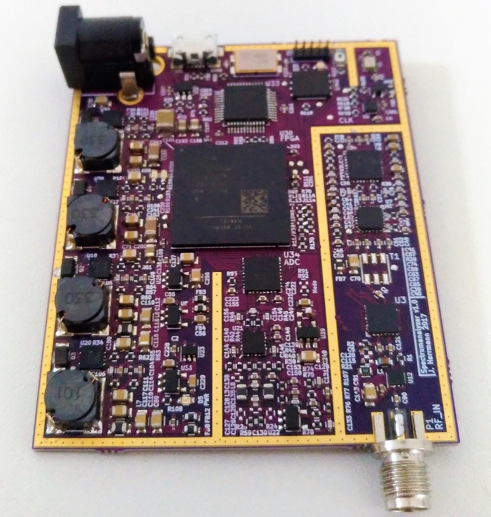
Fig. 2. - Picture of the assembled board.