Dual Microwave Source v2

Schematic Revision

This new revisions builds up on the schematic resources of the Dual Source. The biggest changes in this design, are a more powerful microcontroller and an input for an external clock signal, 
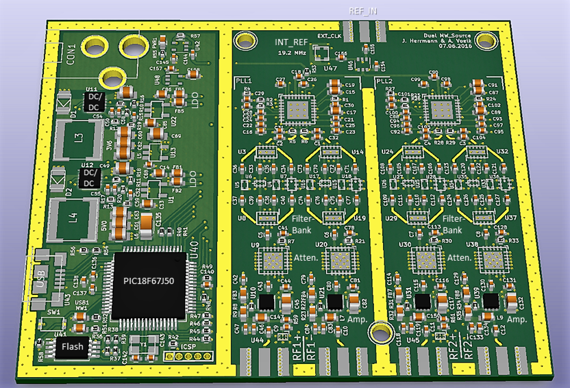
The PIC18F67J50 with its high count of additional I/O pins replaces the old microcontroller with the GPIO expander. Moreover, a new I2C external EEPROM allows the storage of user configuration and calibration data. In order to allow an synchronization of the microwave signals an extra SMA input allows the user to feed in an external clock signal. A subsequent RF-switch allows to switch between the on-baord Local Oscillator (19.2 MHz) and the external input (< 100 MHz).

Fig. 1. - Rendered 3D Model from KiCad.

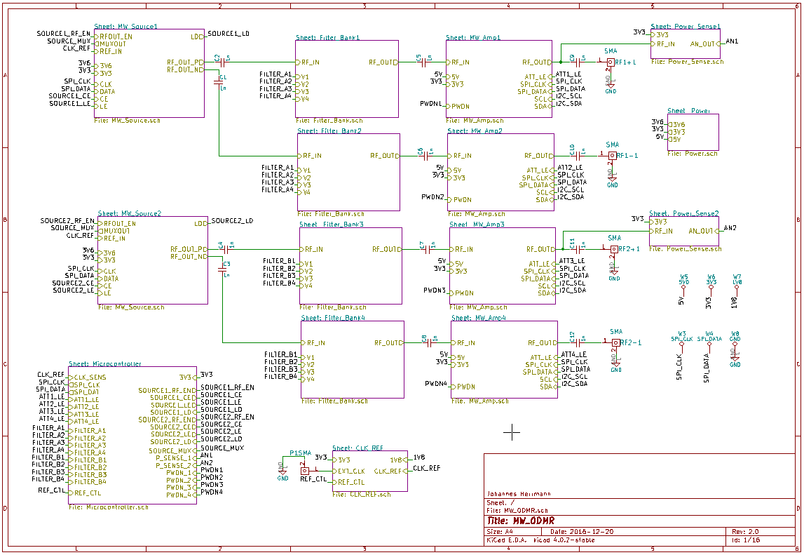
Schematic. Click for PDF.
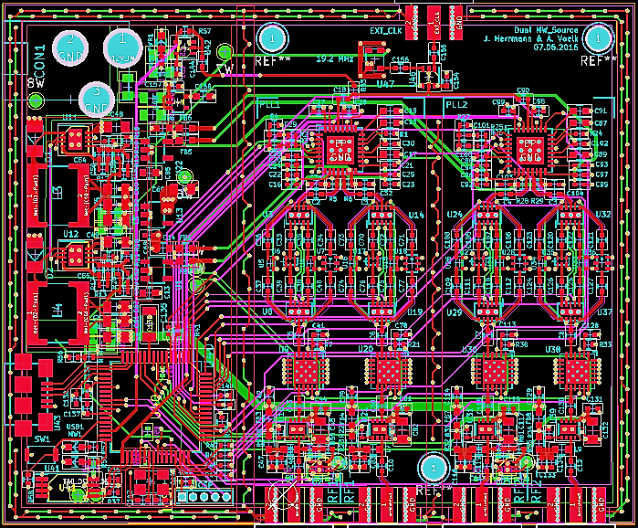
Layout Revision

The new layout includes more space for the RF-traces and an ground shielding around the PCB outline and the two PLLs. Mounting holes for an aluminium case are also provided. Additionally, a 50 Ω matching at the output of the SMA connector for 6 GHz is attained by structuring the underneath ground layer. The geometry of this plane has been verified by a field simulation with CST Microwave Studio®.

Fig. 2. - Board Layout from KiCad.
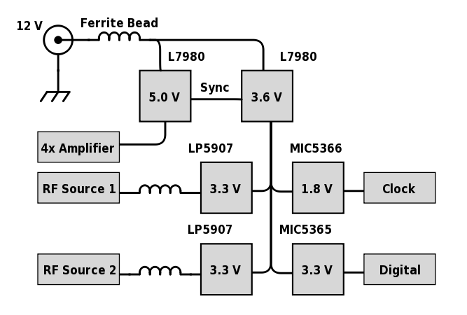
Power Supply Design

The basic power supply system is derived from the components of the Single Source. Here two synchronized step-down switching regulators create two basic voltage rails with 3.6 V and 5.0 V, respectively. To assure a stable noise free supply for both PLLs two seperate ultra-low noise LDOs are used in combination with several ferrite beads. The digital logic is supplied by a common 3.3 V switching regulator. The internal reference clock for the PLL requires an input of 1.8 V which is supplied by a dedicated LDO.

Fig. 3. - Functional Diagram of the Power Supply Design.

New RF Power Detector Circuit

Except of the aforementioned changes, the old RF Power Detector Circuit has been replaced due to problems with its small BGA package and measurement gain. The new Power Detector LTC5532 features a higher precision and controllable gain within a frequency range of 300 MHz to 7 GHz. In order to measure the RF power at the output, an RF-splitter has to be designed. Due to the wide bandwidth requirement, a resistive tap is the best choice here. The coupling factor AdB of this structure can easily be calculated by using th internal impedance RRIN of the detector IC:

A AdB = 20 log(1 + R1/RIN)

The designed circuit aims for a coupling factor of 20dB, which is equivalent to RR1=200 Ω (here RR61). The value of this coupling factor is highly depended on the parasitics and accuracy of the chosen resistor and its geometry in the layout. Luckily the LTC5532 allows an adjustable measurement gain. An additional output pin of this IC (VVm) is a feedback to the inverted input of an internal op-amp. Therefore, the analog gain of the circuit can be controlled by the values of the feedback resistors RR38 and RR61 (AA=1+R61/R38). The capacitor CC150 is a DC-block for the supply voltage of the RF-amplifier on the microwave stripline.

Fig. 4. - Schematic of the RF Power Detector.

PLL Loop Filter Design (LPF)

The basic function of the fractional PLL circuit was discussed in the context of the Single Source. The following section will give a more detailed description of the designed PLL Loop Filter (LPF). A Loop Filter is used to convert the pulsed current output of the Charge Pump to a constant control voltage for the VCO. Therfore, this Filter has a low pass characteristic and additionally suppresses the reference clock frequency and its higher harmonics. Otherwise, unacceptably high spurious tones are present in the PLL output spectrum. Figure 5 shows a part of the schematic related to the MAX2871 PLL. Here, the Loop Filter is marked in blue color and is connected between the CP_OUT and TUNE pin of the PLL chip. The filter connection to the SW pin is only required if the fast lock mode of the PLL is desired.

Fig. 5. - Schematic of the MAX2871 PLL Circuit.

The utilised circuit is a third order filter build from passive RC-components. Figure 6 shows the equivalent circuit diagram of the implementation. The first parallel branch with R1 and C1 transforms the current pulse from the charge pump to a voltage pulse. The subsequent components act as a low pass filter and aim for a constant voltage at the output to the VCO. This can be illustrated by calculating the transfer funtion of the circuit.

Fig. 6. - Third order passive Loop Filter.

The transfer function is calculated by relating the voltage at the VCO to the charge pump current at the input. The resulting term can be isolated according to its poles and nulls in the La Place plane. Where K is the time constant of the integral part and τz the constant which provides a stabilizing zero to the loop. The two poles are determined by the time constants τp1 and τp2 and suppress the tones of the 19.2 MHz reference clock and its higher harmonics.
The absolute value of the transfer function is displayed in Fig. 7. The Bode plot can be sperated into three general regions. The first region is the integral part, which provides the mechanism for the VCO to track the reference clock. A subsequent region of a nearly constant gain ensures stability by providing a big phase margin. In order to supress the high frequency components of the reference clock the last region experiences a big attenuation.

Fig. 7. - Bode Plot of the third order low pass loop filter.

Manufacturing

In order to manufacture the first prototype a stencil for the top size of the PCB has been created. This allows a precise spreading of the solder paste and a subsequent reflow process in a homemade oven leaves us with the first working board.

Fig. 8. - Solder Paste spread on board.

Fig. 9. - Board inside the Reflow Oven.

Fig. 10. - PCB after reflow.

Fig. 11. - First functional test.